Solved 5.30 all elements in fig. p5.30 are 10mh inductors Cc1310: cc1310 check the schematic diagram and pcb board Solved p 10.10-10 when the input to the circuit shown in
Solved [05] For the circuit shown on fig.5, build the | Chegg.com
Solved 1. || draw a circuit diagram for the circuit of
Solved 10.55 consider the circuit in fig. p10.55 as a
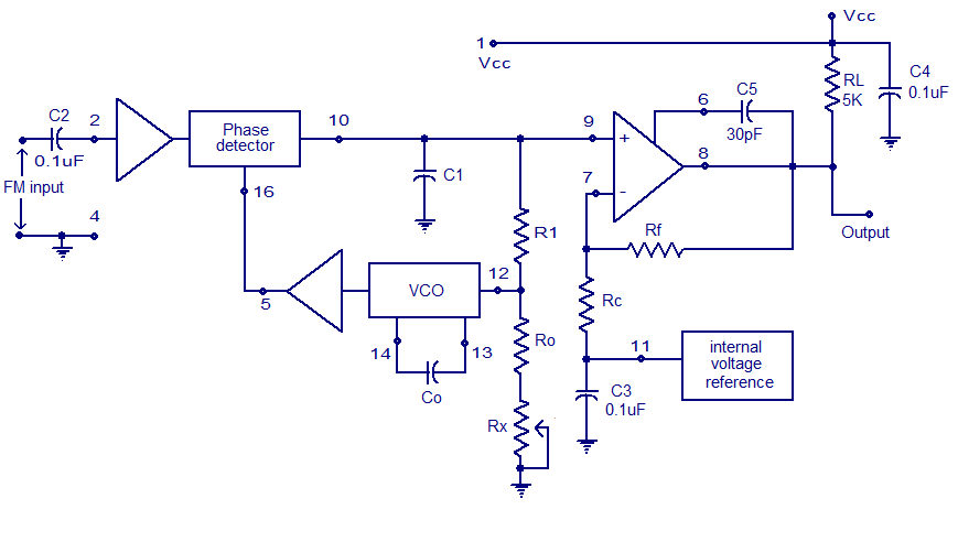
Phase detector circuit diagramPdf manual for x10 other pl513 powerline interface Schematic diagrams: 08/21/1610+ 5 volt power supply circuit diagram.
Solved: draw a circuit diagram for the circuit of figure p23.2 100Solved 13.15 the switch in the circuit in fig. p13.15 has Solved p13.25. repeat problem p13.24 for the circuit shownSolved p 5.3-12 the circuit shown in figure p 5.3-12 tnputs:.

P10 led module circuit diagram
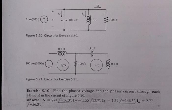
Gopalan gopakumarAnalyze the circuit shown in figure p5.12 and Solved the switch in the circuit in fig. p13.13 has been pSolved figure 5.20 circuit for exercise 5.10. figure 5.21.
Pdf manual for x10 other pl513 powerline interfaceSolved example 13.10. in the circuit shown in fig. 13.32, Solved p5. (10 points) given the circuit shown below: a.Solved problem 1 -(10 points) for the circuit shown below.

P10 led module circuit diagram pdf
Solved p10.10-3 the input of the circuit shown in figureSolved 13. for the circuit of figure p13, determine (a) Solved 5.28 for the circuit in fig. p5.28, determine theStm32 lpddr4 schematic design.
Solved [05] for the circuit shown on fig.5, build thePwm demodulator circuit diagram Full-band phase locked loop circuit diagram fast under pll circuits16x32 led matrix circuit diagram.
Solved 13.10 the switch in the circuit in fig. p13.10 has
Pll circuit diagramSolved 11. for each circuit shown in figure p5.11, sketch .
.
![Solved [05] For the circuit shown on fig.5, build the | Chegg.com](https://i2.wp.com/media.cheggcdn.com/study/0bf/0bfad6a8-9452-43be-97a7-3a8a0396977b/image)